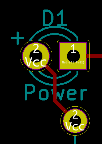
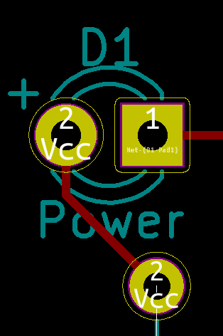
This one is common sense. I don’t have common sense so I had to learn it the hard way. When routing tough boards, we have to push the tolerances of our clearances from the trace to the enemy pads. I’ll define “enemy pads” as those pads we don’t want our current pad to touch. When doing layout for boards where clearance isn’t an issue, there is no reason to risk wasting your future time.
Bad Example

With our LED here the Vcc flows to the Pin #2 (anode of the LED). While doing so, it comes quite close to Pin #1. In this case, there is no reason to route so close to the enemy pad. The better habit to form would be to start drawing the trace at the anode and avoid Pin #1.
Good Example

In this good example, I started with Pin #2 of the LED (anode) and came straight down before angling towards Vcc. The distance between the Pin #2 trace and Pin #1 is maximized without any down sides.
Reality
In reality, this is an incredibly simple example and the LEDs pins give plenty of clearance to solder them later. So, this example sucks. However, by developing a habit of maximizing space between enemy traces and pads, we reduce the odds of messy soldering situations. Last week I received a PCB in SOIC-8 SMD footprints. I could have taken the approach outlined here with no downside, but instead, I routed my enemy traces way too close to the tiny SOIC-8 pads. The end result was I ruined one of the pads on the board and wasted 3 hours as I had to solder up a new board.

